Double Layer PCB

      Rs

      Description


      Double Layer PCB: Superior Performance and Reliability

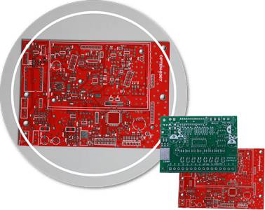
      Our Double Layer Printed Circuit Boards (PCBs) offer a reliable and cost-effective solution for a wide range of electronic applications. Perfect for projects requiring moderate complexity and density, these PCBs provide a balance between functionality and affordability. This description details the key features, benefits, and specifications of our double-layer PCBs.

      Key Features:

      • Two Copper Layers: Provides improved signal integrity and reduced crosstalk compared to single-layer boards. This allows for more complex designs with higher component density.
      • FR-4 Material: Utilizing high-quality flame-retardant FR-4 substrate ensures durability, stability, and compliance with industry safety standards.
      • Various Finishes: Choose from a range of surface finishes including HASL (Hot Air Solder Leveling), ENIG (Electroless Nickel Immersion Gold), and OSP (Organic Solder Preservative) to optimize solderability and longevity. Specific finish options affect cost and performance – consult our specifications for details.
      • Customizable Design: We offer complete design flexibility. You can provide your Gerber files, or our experienced engineers can assist with your design needs. We support a wide range of component footprints and design requirements.
      • Precise Manufacturing: State-of-the-art manufacturing processes ensure precise trace widths, spacing, and overall board quality, minimizing errors and maximizing reliability.
      • Various Board Sizes: Available in a range of standard and custom sizes to fit your specific project needs.
      • Quick Turnaround Time: We offer competitive lead times to meet your project deadlines efficiently.

      Benefits:

      • Increased Component Density: The double layer allows for a greater number of components to be placed on the board, minimizing the overall size and cost of your product.
      • Improved Signal Integrity: Reduced crosstalk and improved signal routing contributes to better performance and stability of your electronic device.
      • Enhanced Reliability: High-quality materials and manufacturing processes ensure long-term durability and reliability under various operating conditions.
      • Cost-Effective Solution: Double-layer PCBs offer a balance between performance and cost, making them ideal for a broad range of applications.
      • Flexibility and Customization: Tailor your PCB to your specific needs with our flexible design and manufacturing capabilities.

      Applications:

      Double-layer PCBs are suitable for a wide variety of applications including:

      • Consumer Electronics: From simple gadgets to more sophisticated devices.
      • Industrial Control Systems: Reliable and robust boards for industrial applications.
      • Automotive Electronics: Meeting the stringent requirements of the automotive industry.
      • Medical Devices: Suitable for certain medical device applications (specific regulatory compliance may need to be considered).
      • Prototyping and Development: Ideal for testing and developing new electronic products.

      Specifications:

      (Note: Specific specifications may vary depending on the chosen options. Please consult our data sheets for detailed information.)

      • Material: FR-4 (other materials available upon request)
      • Thickness: Various thicknesses available (e.g., 1.6mm)
      • Minimum Trace Width & Spacing: Specify during design phase
      • Surface Finish: HASL, ENIG, OSP (other finishes available upon request)
      • Drill Size: Specify during design phase
      • Impedance Control: Available upon request (add-on cost applies)

      Ordering Information:

      To order your custom double-layer PCBs, please provide the following:

      • Gerber files: Your complete design files in Gerber format.
      • Bill of Materials (BOM): A list of components used in your design.
      • Quantity: The number of PCBs required.
      • Surface finish: Your preferred surface finish.

      Contact us today for a quote and lead time estimation! We are happy to assist you with any questions you may have.

      Seller Details

      PCB GLOBE INDIA PVT. LTD.

      Gandhinagar, gujarat

      ["Manufacturers","Service Providers"]

      Looking for Best Price

      Tags: Double Layer PCB