Description
Polycrystalline Technology: A Deep Dive
Polycrystalline technology, often shortened to polysilicon, is a fundamental manufacturing process used to create various electronic components, most notably solar cells and integrated circuits. Unlike its monocrystalline counterpart, polycrystalline materials aren't composed of a single, continuous crystal lattice. Instead, they consist of numerous smaller crystals, each with a slightly different orientation, fused together. This difference in structure significantly impacts the material's properties and resulting applications.
Understanding the Structure and Properties
The "poly" in polycrystalline refers to the multiple crystalline structures within the material. These individual crystals are randomly oriented, resulting in grain boundaries where these crystals meet. These grain boundaries affect the material's properties, making it slightly less efficient than monocrystalline silicon in some applications, but also offering advantages in terms of cost and manufacturing process.
Key Properties of Polycrystalline Materials:
- Lower Cost: Polycrystalline silicon is significantly cheaper to produce than monocrystalline silicon. This is due to a simpler and less energy-intensive manufacturing process. The energy savings contribute to a lower carbon footprint per unit produced.
- Slightly Lower Efficiency: The grain boundaries in polycrystalline silicon act as minor impediments to electron flow, resulting in slightly lower energy conversion efficiency compared to monocrystalline silicon in solar cells. However, advancements in manufacturing techniques have significantly narrowed this gap.
- Easier Manufacturing: The manufacturing process for polycrystalline silicon is less demanding than monocrystalline silicon, allowing for higher production volumes and greater scalability. This makes it a more accessible material for mass production.
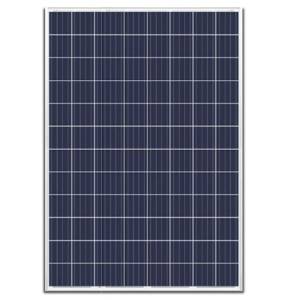
- Variable Appearance: Due to the variations in crystal orientation, polycrystalline materials often exhibit a mottled or speckled appearance, unlike the uniform appearance of monocrystalline materials.
Applications of Polycrystalline Technology:
Polycrystalline technology finds its primary applications in:
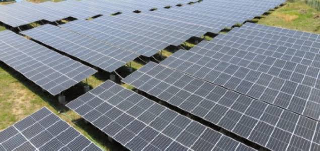
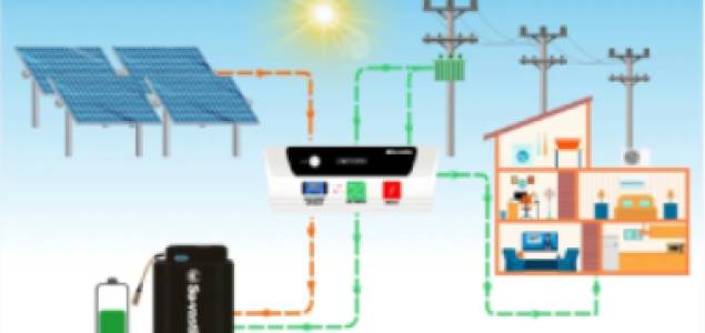
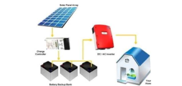
- Solar Cells: Polycrystalline silicon is widely used in photovoltaic (PV) solar cells, offering a cost-effective alternative to monocrystalline solar cells. While slightly less efficient, the lower manufacturing cost makes it a highly competitive option for large-scale solar power generation.
- Integrated Circuits (ICs): Although less common than monocrystalline silicon in high-performance ICs, polycrystalline silicon is used in some applications where high purity isn't critical, such as in thin-film transistors (TFTs) found in LCD screens and some solar cells.
- Other Applications: Polycrystalline materials are utilized in various other applications, including:
- Metallization layers in microelectronics.
- Certain types of sensors.
- Polycrystalline diamond films for wear-resistant coatings.
Advantages and Disadvantages Summary:
Advantages:
- Lower cost
- Easier and faster manufacturing process
- Higher production volumes
- Environmentally friendlier (lower energy consumption during production)
Disadvantages:
- Slightly lower efficiency compared to monocrystalline silicon
- Less uniform appearance
Conclusion:
Polycrystalline technology represents a significant advancement in materials science, providing a cost-effective and scalable solution for various applications. While offering slightly lower performance in certain areas compared to monocrystalline materials, its advantages in cost, scalability, and environmental impact make it a crucial technology for numerous industries, particularly in renewable energy generation. Continuous advancements in manufacturing processes are further enhancing its efficiency and expanding its applications.